A primer on ‘flip chip’ manufacturing techniques for smart card ICs
24 May, 2005
category: Library
 Editor’s preface: There is increasing interest in the ‘new’ smart card chip manufacturing technique known as Flip Chip. An alternative to the tradional manufacturing process that attached chips to substrates via tiny wire bonds, flip chip offers a number of benefits and efficiencies. To get a better understanding of the process, SecureIDNews asked one of the leaders in the field, Dr. George Riley, a man known to many as Dr. Flipchip, to develop a primer on the technology and its use with smart cards and RFID.
By George A. Riley, PhD, FlipChips Dot Com
As technology life spans go, flip chip interconnection should by now be doddering to its grave. Instead, it is still growing like an adolescent. Let me explain what’s behind this age-defying technology’s eternal youth.
Flip chip was born at IBM in the early 1960s, to support their now-dinosaur mainframe computers. GM developed their version of flip chip for automotive electronics in the 1970s, and now use over 300,000 flip chips a day. The first consumer flip chip products appeared as cheap calculators in the early 1990s, followed closely by inexpensive digital watches. Since then, flip chip has blossomed into today’s cell phones, hearing aids, digital cameras, PDA, pagers and many other portable devices. Over the past decade, flip chip has also become the preferred assembly method for hundreds of millions of smart/RFID cards annually.
WHAT?
Flip chip assembly is the direct electrical connection of face-down (hence, “flipped”) electronic components onto substrates, circuit boards, or other components, by means of conductive bumps on the chip bond pads. In contrast, wire bonding, the older technology that flip chip replaces, uses face-up chips with an individual wire connected to each bond pad. Figure 1 is a conceptual view of a flip chip and substrate.
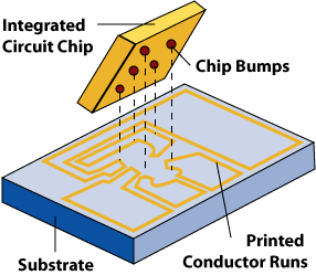
FIGURE 1. A flip chip and substrate, shown with the bumped active face of the die to be placed face down upon the matching substrate.
Flip chip was first used with semiconductor devices. Now semiconductors, passive components, antennas, sensors, optical and electromechanical devices are all assembled in flip chip form. Flip chip is also called Direct Chip Attach (DCA), a more descriptive term, since the chip is directly attached to the substrate, board, or carrier by the conductive bumps.
WHY?
The continuing boom in flip chip packaging results from flip chip’s advantages in size, performance, flexibility, reliability, and cost over other microelectronic assembly methods.
Smallest Size – Eliminating bond wires and cumbersome individual packages reduces the required board area per chip by up to 95% and the height by more than 50%. Weight can be less than 5% of the packaged device weight. Flip chip is the simplest minimal package, smallest because it is very close to chip size.
Highest Performance – Because of its small size, flip chip offers the highest speed electrical performance of any assembly method. Eliminating bond wires reduces the delaying inductance and capacitance of the connection by a factor of 10, and shortens the signal path by a factor of 25 to 100. The result is high speed off-chip interconnection.
Greatest Connection Flexibility – Flip chip gives the greatest input/output connection flexibility. Wire bond connections are limited to the perimeter of the die, driving die sizes up as the number of connections increases. Flip chip connections can use the whole area of the die, accommodating many more connections on a smaller die, and placing them most efficiently. Area connections also allow 3-D stacking of die and other components.
Most Rugged – Flip chip is mechanically the most rugged interconnection method. Flip chips, when completed with an adhesive “underfill,” are solid little blocks of cured epoxy. They have survived laboratory tests simulating the forces of rocket liftoff and of artillery firing, as well as millions of cumulative total hours of actual use in computers and under automobile hoods.
Lowest Cost – Flip chip can be the lowest cost interconnection for high volume automated production, with costs of a fraction of a cent per connection. This explains flip chip’s longevity in the cost-conscious automotive world, and growing popularity in smart cards, RFID cards, cellular telephones, and other cost-dominated applications.
HOW?
There are three steps in making a flip chip connection: putting conductive bumps on the die bond pads, attaching the bumped die to matching pads on the board or substrate, and filling the remaining space under the die with a protective, electrically non-conductive adhesive. The conductive bump composition, the attachment materials, and the assembly processes used differentiate the many varieties of flip chip assemblies. The cost, performance, and space constraints of the application determine which flip chip process is the best solution. We’ll focus here on gold-bumped adhesive assembly, one of the most practical flip chip bumping and attaching methods for smart cards/RFID.
Gold bumps may be deposited by plating, sputtering, or direct bonding. Plated gold bumps require pre-processing to remove the insulating aluminum oxide before plating gold bumps onto the wafer bond pads. Plated nickel-gold bumps are formed on the semiconductor wafer by electroless plating of the aluminum bond pads of the chips. After plating the desired thickness of nickel, a gold layer is added, and the wafer is sawn into bumped die. Alternatively, pure gold bumps may be electroplated onto processed bond pads before sawing, or gold stud-bumps may be directly mechanically placed on the pads using gold wire in a ball-bonder.
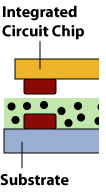
The preferred adhesive assembly method for smart cards/RFID goes by the mouth-filling name of “anisotropic conducting film,” or ACF. ACF consists of millions of microscopic conductive spheres distributed uniformly throughout a non-conductive polymer adhesive film. The spheres have a thin outer insulating layer, and are normally not touching each other, so the film is an electrical insulator. Figure 2 gives a conceptual view of ACF film before assembly.
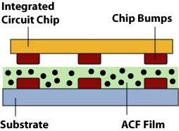
FIGURE 2. ACF film before assembly, with the spheres uniformly distributed and making no electrical conducting paths.
In the ACF assembly process, heat softens the film, while pressure forces the die and substrate bond pads together, trapping some conductive spheres between them and breaking through the sphere insulation to form conducting paths from die to substrate pads. Cooling the film locks the pads and trapped conducting spheres in position, while non-trapped insulated spheres remain distributed, with no electrical contacts. Figure 3 is a conceptual view of the ACF film after assembly. The entire ACF assembly operation is carried out by high-speed automated equipment, for high throughput and low cost.
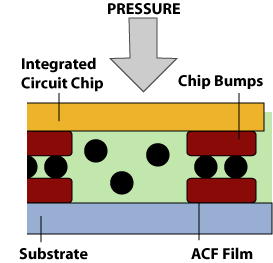
FIGURE 3. ACF film after assembly, with the conducting spheres locked between the chip and substrate bond pads.
The non-conducting ACF film also acts as the “underfill” adhesive, filling all of the space under the die to lock together and protect the die and substrate. Because cured ACF conducts only in the vertical, pad-to-pad direction, it is sometimes called “Z-axis” film. ACF has been used commercially since 1992, and now provides billions of interconnections per year, including hundreds of millions of smart cards/RFID.
CONCLUSION
Flip chip in general is still growing at 30% to 40% per year, and could have a long and happy life for high volume, low cost, smart card/RFID assembly. As always with micropackaging technologies, smaller and possibly less costly contenders are creeping out of the laboratories. Leading candidates now include the nanotechnology family. Possibilities include nanofilms, a version of ACF with aligned conductive filaments replacing distributed conducting spheres, and nanoparticle adhesives with uniquely improved behaviors. Will flip chip be the champion in smart card/RFID a decade from now? Only time and cost will tell.
FOR FURTHER INFORMATION
- To learn more about flip chip processes, visit www.flipchips.com
- To learn more about nanofilms, visit www.www.btechcorp.com
- To learn more about nanoparticle adhesives, visit www.nanodynamics.com.


